- Jintu K Joseph
- April 9, 2025
A Complete Guide to SoC Debugging | Part 2
In modern System-on-Chip (SoC) designs, a debugger is connected to the SoC via dedicated debug interfaces that allow developers to access and control internal components for debugging, testing, and programming. The two most common debug interfaces are JTAG (Joint Test Action Group) and SWD (Serial Wire Debug).
JTAG interface for debugger
JTAG or Joint Test Action Group was developed in 1980 to improve the testing and debugging of digital circuits. JTAG is defined by the Institute of Electrical and Electronic Engineers (IEEE) 1149.1 JTAG is a standard interface used to test and debug integrated circuits.

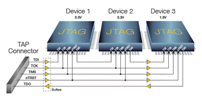
Test Access Port (TAP) is a controller that handles a set of pins that provide access to the JTAG circuits. The TAP consists of 5 signals. TAP controller has a state machine inside, it is responsible for interpreting the TCK, and TMS signals. The data input pin is used for loading data into the boundary scan cells, between the physical pin and the IC core.
The JTAG signals are
- Test Clock (TCK)
- Test Mode Select (TMS)
- Test Data Input (TDI)
- Test Data Output (TDO)
- Test Reset (TRST)
There are two modes the JTAG controller state machine can support.
- Instruction Mode
- Data Mode
State transitions are controlled by the TMS signal. The JTAG state machine is given below.

IR (Instruction Register) is a shift register that stores instructions for the JTAG circuits. The length of the IR is determined by the number of instructions that the JTAG circuitry supports. Data Register (DR) contains a set of registers like design-specific registers, Device ID registers, Bypass registers, boundary scan registers etc.

The primary function of a JTAG/Serial Wire Debug Port is to convert serial scan transactions into bus transactions. JTAG is more than debugging and programming, The boundary-scan test architecture provides a means to test interconnects between integrated circuits on a board without using physical test probes.
It is a multi-mode (synchronous) serial port. JTAG is commonly used for debugging embedded systems and microcontrollers. It provides a way to stop the processor’s operation, examine the contents of registers and memory, and control the execution of code step by step. This is crucial for finding and fixing software bugs and hardware issues in embedded systems. JTAG can be used to program firmware and configuration data onto programmable logic devices (FPGAs) and microcontrollers. It offers a standardized way to load software onto these devices during production or field updates. JTAG employs a standardized pinout and communication protocol, which makes it compatible across different manufacturers and devices. This ensures that debugging tools and equipment can work across a wide range of hardware.
SWD Interface for debugger
Serial Wire Debug (SWD) provides a debug port for severely pin-limited packages, often the case for small package microcontrollers but also complex ASICs where limiting pin count is critical and can be the controlling factor in device costs. SWD replaces the 5-pin JTAG port with a clock + single bi-directional data pin, providing all the normal JTAG debug and test functionality plus real-time access to system memory without halting the processor or requiring any target resident code. SWD uses an Arm standard bi-directional wire protocol, defined in the Arm Debug Interface v5, to pass data to and from the debugger and the target system in a highly efficient and standardized way. SWDIO and SWCLK are overlaid on the TMS and TCK pins.
The Arm Serial Wire Debug Interface uses a single bi-directional data connection. The serial interface can provide a separate clock connection, and transfer data synchronously, or transfer data asynchronously, for minimum pin count. However, only the synchronous connection option is used.
Each successful SWD transfer consists of 3 parts:
- A header (always from the external debugger)
- An acknowledgement from the target (provided it recognises the header)
- A data payload, the direction of which is determined by the header.
A write transfer is shown in the Figure below.

A read transfer is shown in the Figure below.

Key features of SWD
- Start — A single start bit, with value 1.
- APnDP — A single bit, indicating whether the Debug Port or the Access Port Access Register is to be accessed. 1 for accessing AP.
- RnW — A single bit, this bit is 0 for a write access or 1 for a read access.
- A[2:3] — Two bits, giving the A[3:2] address field for the DP or AP register address.
- Parity — A single odd parity bit is made over the APnDP, RnW and A[2:3] bits.
The number of bits set to 1 is odd, then the parity bit is set to 1. - Stop — A single stop bit. In the synchronousSWD protocol, this is always 0.
- Park — A single bit, with value 1.
- Trn — The turn-round cycle (TRN in the diagrams) is placed after the data phase for a read, as there is no change of direction between ACK and RDATA. Every time the SWDIO changes data direction, a one-cycle turnaround period is inserted which both sides should ignore.
- OK, Response — It indicates successful operation, value is b001. : SWD Line: 1 0 0
- WAIT response — The host must retry the operation later, value is b010. : SWD Line : 0 1 0
- FAULT response — If the target responds with FAULT, an error has occurred and one of the sticky bits in CTRL/STAT is set.

JTAG to SWD switching
SWJ-DP is a specialised IP, that enables either an SWD or JTAG protocol to be used on the debug port. To do this, it implements a watcher circuit that detects a specific 16-bit selection sequence on the SWDIOTMS pin:
The 16-bit JTAG-to-SWD select sequence is defined to be 0b0111100111100111, MSB first. This can be represented as 16’h79E7 if transmitted MSB first or 16’hE79E if transmitted LSB first.
Before using the SW-DP an initialization sequence must be performed to establish communication and bring the SW-DP to a known state.
- Send more than 50 SWCLKTCK cycles with SWDIOTMS=1. This ensures that both SWD and JTAG are in their reset states.
- Send the 16-bit JTAG-to-SWD select sequence on SWDIOTMS
- Send more than 50 SWCLKTCK cycles with SWDIOTMS=1. This ensures that if SWJ-DP was already in SWD mode, before sending the select sequence, the SWD goes to line reset.
- Perform a READID to validate that SWJ-DP has switched to SWD operation.
Open-Source vs. Proprietary On-Chip Debug Frameworks:
Debugging is a critical part of System-on-Chip (SoC) development, ensuring proper functionality, performance optimization, and issue resolution. Two major on-chip debug frameworks are:
- OpenSoC Debug – An open-source, modular debug infrastructure, Open SoC Debug is an open-source project aimed at providing a standardized infrastructure for debugging System-on-Chip (SoC) designs. CoreSight™ is a proprietary technology developed by Arm, providing comprehensive debug and trace capabilities for Arm-based systems. Both provide flexible solutions, but CoreSight™ offers more advanced features tailored for Arm-based systems. Open SoC Debug is ideal for those seeking an open-source, community-driven solution, while Arm CoreSight™ provides a comprehensive, proprietary solution with advanced features and vendor support. Open SoC Debug is co-managed by the OpTiMSoC and lowRISC projects. Here are some key points about Open SoC Debug:
- Arm CoreSight – Arm’s proprietary, industry-standard debug & trace framework. CoreSight is Arm’s on-chip debug and trace technology that provides efficient debugging & real-time performance monitoring in Arm-based SoCs.

How will Arm's CoreSight™ solve the above challenges?
CoreSight is the name of the on-chip debug and trace technology provided specially by Arm for multicore processors. The Arm Debug Interface (ADI) defines the interface for debug components in an embedded SoC. The CoreSight Base System Architecture (CoreSight-BSA) defines the hardware system architecture for debug functionality. It enables standard software – operating systems, debugging and performance optimization software – to work seamlessly across compliant devices.
Arm CoreSight™ offers a variety of packages designed to provide comprehensive debug and trace capabilities for different system configurations. Here are some of the key CoreSight™ packages:
- CoreSight™ SoC-400: This package includes a set of components for implementing debug and trace functionality in System-on-Chip (SoC) designs. It provides a scalable and flexible solution for integrating debug and trace features into complex SoCs.
- CoreSight™ SoC-600: An advanced version of the SoC-400, the SoC-600 package offers enhanced features and improved performance for debugging and tracing in modern SoC designs. It includes support for high-speed trace and advanced debug capabilities.
- CoreSight™ ELA-500: The Embedded Logic Analyzer (ELA) package provides real-time visibility into the internal operations of an SoC. It allows developers to capture and analyze complex events and interactions within the chip.
- CoreSight™ TMC: The Trace Memory Controller (TMC) package includes components for managing trace data storage and retrieval. It supports various trace storage configurations, including on-chip and off-chip memory.
- CoreSight™ CTI: The Cross Trigger Interface (CTI) package enables cross-triggering between different debug and trace components. It allows for synchronized debugging and tracing across multiple cores and subsystems.
- CoreSight™ ETM: The Embedded Trace Macrocell (ETM) package provides instruction trace capabilities for capturing the execution flow of software running on the processor. It is essential for detailed performance analysis and debugging.
- CoreSight™ ITM: The Instrumentation Trace Macrocell (ITM) package offers real-time trace capabilities for capturing software events and data. It is useful for monitoring and debugging real-time systems.
- CoreSight™ STM: The System Trace Macrocell (STM) package provides system-wide trace capabilities for capturing events and data from various sources within the SoC. It is ideal for system-level debugging and performance analysis.
The debug architecture, such as Arm’s CoreSight™, plays a significant role in addressing some of the issues in SoC design. Here’s how:

Power Consumption
- Real-Time Monitoring: CoreSight™ enables real-time power monitoring and profiling, which helps in identifying power-hungry components and optimizing their usage.
- Low-Power Debug: CoreSight™ supports low-power debug modes, allowing developers to debug without significantly impacting power consumption.
Design Complexity
- Real-Time Monitoring: CoreSight™ enables real-time power monitoring and profiling, which helps in identifying power-hungry components and optimizing their usage.
- Low-Power Debug: CoreSight™ supports low-power debug modes, allowing developers to debug without significantly impacting power consumption.
Verification and Testing
- Comprehensive Trace: Provides extensive trace capabilities to capture detailed execution flow, which is crucial for thorough verification and debugging.
- Breakpoint and Watchpoint: CoreSight™ allows setting breakpoints and watchpoints to isolate and investigate specific issues during testing.
Performance
- Performance Monitoring: Enables performance counters and monitoring features to identify and optimize performance bottlenecks.
- Profiling: Provides detailed profiling of system behaviour, helping to balance performance with power efficiency.
Security
- Secure Debug Access: CoreSight™ includes features for secure debug access, ensuring that only authorized personnel can access the debug interface.
- Tamper Detection: Supports tamper detection and response mechanisms to protect against unauthorized access and security threats.
Integration
- Standard Protocols: Uses standardized debug and trace protocols, ensuring compatibility and ease of integration with various IP blocks.
- Scalable Debug Solutions: Offers scalable solutions that can be tailored to different SoC configurations, from simple to complex designs.
Signal Integrity
On-Chip Trace: Minimizes the need for external probes, reducing signal integrity issues associated with high-frequency signals.
Overall, a robust debug architecture like CoreSight™ helps in identifying, analyzing, and resolving various issues during SoC design and development, leading to a more efficient and reliable system.
If you haven’t already, be sure to check out the previous blog in the series, A Complete Guide to SoC Debugging – Part 1: Understanding the Debug Architecture of ARM-based SoCs, to build a solid foundation— and stay tuned for the next installment, Part 3: CoreSight-Based SoC Debug, where we’ll dive into how ARM CoreSight technology enables efficient, scalable debug and trace capabilities in complex SoC environments.