- Jintu K Joseph
- April 23, 2025
A Complete Guide to SoC Debugging | Part 3
Introduction
CoreSight-based debugging is a powerful infrastructure from Arm that provides visibility into the inner workings of complex SoCs. From trace collection to real-time monitoring, CoreSight offers developers the tools to pinpoint issues with precision and efficiency.
Debug architecture
A debug architecture typically includes:
- Debug modules: Monitor or interact with the SoC’s functional components. These modules are self-describing and discoverable at runtime.
- Debug interconnect: Exchanges data between debug modules, and between the target and the host.
- Physical transport: Connects the target to the host.
- Debug access port (DAP): Provides a connection from the designer’s debug environment to the SoC under test. An SoC may have multiple DAPs.
JTAG interface for debugger
- Breakpoints: to stop the execution of the SoC at a specified location
- Watchpoints: to monitor the value of a specified variable or memory location.
- Single stepping: to execute the SoC one instruction at a time.
- Run control: to start, stop, or resume the execution of the SoC.
JTAG interface for debugger
- Integrated development environments (IDEs): to provide a comprehensive set of tools for coding, compiling, debugging, and testing your SoC.
- Logic analysers: to capture and display the digital signals of your SoC.
- Oscilloscopes: to measure and display the analogue signals of your SoC.
- Protocol analysers: to decode and display the data packets of your SoC’s communication protocols.
- Emulators: to emulate the behaviour of your SoC on a hardware platform.
- In-circuit debuggers (ICDs): to connect your SoC to a host computer or device via a cable or wireless connection.
Arm Debug interface
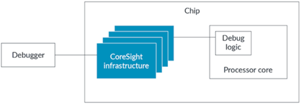
For the external component to access the built-in debug capability of the processor, a debug infrastructure must be built into the chip. This infrastructure provides the connectivity between the debugger and the processor. The mechanism that Arm uses to provide this debug infrastructure is based on the CoreSight™ architecture. The following diagram illustrates the CoreSight™ infrastructure concept:
A common debug activity is to halt a processor core, by stopping the execution of the program and allowing an external debugger to check the status of the processor core registers.
Arm Development Studio [DS]: Designed specifically for the Arm architecture, Development Studio is the most comprehensive embedded C/C++ dedicated software development solution with support of multicore debugging for Cortex-A, Cortex-R, Cortex–M, and Neoverse Arm CPUs. Uniquely it provides the earliest support for all the latest CPUs and interconnects. Primarily the Arm Debugger is used for validation of SoCs through emulation, simulation, FPGA, and silicon bring-up.
The Arm Debug Interface Architecture (DIA) specification defines a standard debugging interface between debug agents and Arm processor cores. This allows debugging agents from various vendors to connect to and debug Arm cores without needing core-specific knowledge. The DIA provides a consistent method for accessing debug features like breakpoints, watchpoints, and register access across Arm cores. CoreSight-400 and CoreSight-600 provide components to build and validate the debug and trace elements of an SoC built with Arm processors. The components are grouped into categories as follows:
- Controlling and accessing components,
- Trace sources,
- Trace links,
- Trace sinks,
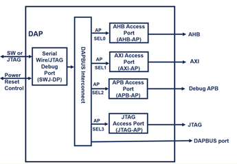
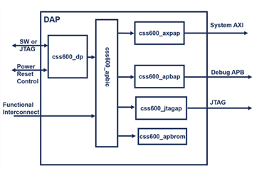
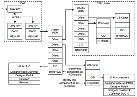
CoreSight devices are behind a CoreSight Debug Access Port (DAP). The DAP is an implementation of the Arm Debug Interface Architecture Specification. A DAP is a Debug Port (DP) that is connected to one or more Access Ports (APs). The Debug Port can be used to configure transactions and read or write to one or more Access Ports (AP). An Access Port exposes an interface to different parts of the MCU. A DP provides a connection from outside the SoC to one or more APs. Usually, the connection is based on a simple physical interface like JTAG or Serial Wire (SW).
The ADI [Arm Debug interface] and CoreSight SoC versions implemented determine the DP version that is used. The DAP spec defines three different protocols which can be used to expose an interface from the Debug Port to the outside world.
- JTAG Debug Port (JTAG-DP) – Based on the IEEE 1149.1 Standard for Test Access Port (TAP). This debug interface requires the MCU to expose at least 4 pins and one optional pin (DBGTRSTn). At its core, the protocol operates on a sequence of shift registers and a fairly complex state machine to push data in / get data out.
- Serial Wire Debug (SWD) Port (SW-DP) – SWD was designed to reduce the number of physical pins that need to be exposed. One pin, SWDIO, is used for input/output and the other SWCLK is used for clocking data in and out. Sampling of SWDIO is performed on the rising edge of the clock.
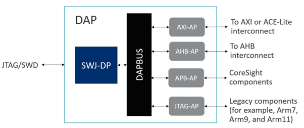
- Serial Wire/JTAG Debug Port (SWJ-DP) SWJ-DP is the best of both worlds and exposes an interface where JTAG or SWD can be used. DAP here is configured with a combined serial wire JTAAG external interface and APB internal debug access.
The Arm Debug Interface (ADI) has evolved through several versions, each introducing new features and improvements. Here are the main versions:
- ADIv1 and ADIv2: Implemented on the ARM7TDMI and ARM9 families of processor cores. These versions are based on the IEEE 1149.1 JTAG interface and were primarily used for accessing Arm processor cores and Embedded Trace Macrocells (ETMs).
- ADIv3: Introduced for the ARM10 processor family. This version continued to use the JTAG interface but included enhancements for better performance and functionality.
- ADIv4: The first version is to be linked with an Arm architecture version (ARMv6) rather than a specific processor core implementation. ADIv4 introduced more flexibility and improved debug capabilities.
ADIv5: The latest major version, which removes the link between the ADI and specific Arm processor cores. ADIv5 can access any debug component that complies with the ADIv5 specification. It supports both the IEEE 1149.1 JTAG interface and a low pin count Serial Wire interface, offering greater versatility and efficiency.
Coresight Debug Access Port
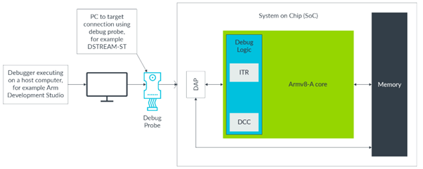
In the external debug model, Debug registers are accessed using the external debug interface. This means the external debug interface is implementation-defined. However, most ARMv8-A systems include a Debug Access Port (DAP) to access the external debug interface for off-chip external debuggers. DP[Debug ports] and AP [Access Ports] are collectively known as DAP. DP is a master device which implements the external interface. Debug ports supporting both JTAG and optimized 2-pin Serial Wire interface. Debug port access from the external debugger is performed as a 32-bit (word) read-or-write transaction targeting either DP registers or AP registers. Each DAP contains between 1 and 256 Aps. The APs are controlled by the DP in response to the external commands.
ADIv5.x and ADIv6 define two pairs of power control signals in the DP CTRL/STAT register:
- CDBGPWRUPREQ and CDBGPWRUPACK. CDBGPWRUPREQ is a signal from the debug interface to the power controller to fully power the system and ensure that clocks are available to the debug power domain. This ensures that the debugger can access enough debug resources of the CoreSight devices to perform basic debug operations, such as halting the processor, accessing registers, or reading trace data, even when the rest of the system may be powered down.
- CSYSPWRUPREQ is a signal from the debug interface to the power controller to fully power the system and ensure that clocks are available to the system power domain. This ensures that the debugger can access the non-CoreSight components of a SoC, like main memory and interconnects.
These signals are requests to the system power and clock controller to enable external debugging. The system power and clock controller should honour these requests.
The Debug Access Port (DAP) manages the low-level operations of the physical debug interface protocol. It exposes a set of memory-mapped registers that a debug agent can use to detect, configure, and interact with the target system. The DAP is compatible with both JTAG and SWD as transport interfaces.
Key capabilities provided by the DAP include:
- Interface identification and capabilities discovery
- Target device identification
- Managing resets and power modes
- Accessing AP/DP registers on the target system
- Handling async events from target
Access Port
An Access Port (AP) is an interface connected to a Debug Port (DP) or debug link, serving as a bridge to access other components within the SoC. In ADIv5, a single DP can support up to 256 APs, while in ADIv6, the number of supported APs is limited only by the available address space.
- A Memory Access Port (MEM-AP) provides a window into a memory system.
- Advanced Peripheral Bus Access Port (APB-AP), For interfacing with APB memory systems
- Advanced High-performance Bus Access Port (AHB-AP), For interfacing with AHB memory systems.
- Advanced extensible Interface Access Port (AXI-AP), For interfacing with AXI memory systems.
- JTAG Access Port (JTAG-AP), For interfacing with legacy components like pre-CoreSight processors. For example, ARM7, ARM9, and ARM11 processors.
The debug registers within processor cores, as well as those in CoreSight components such as the Cross Trigger Interface (CTI), are typically accessed over buses that use the APB (Advanced Peripheral Bus) protocol. Consequently, an APB Access Port (AP) is used to reach these debug control registers.
For Cortex-M processors, debug registers are accessed via the AMBA AHB (Advanced High-performance Bus) interface. This requires an AHB Access Port for performing debug operations on a Cortex-M processor.
When a debugger needs to access memory, it can do so in two main ways:
- By issuing direct transactions to a Cortex-M processor’s memory space using the AHB Access Port, or
- For A-profile processor cores, by interacting with their debug registers to instruct the core to access the memory on the debugger’s behalf.
Access port control
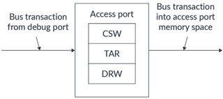
There are three main registers that the external debugger can use to generate accesses into the memory space of an access port:
- Control/Status Word (CSW)
- Transfer Address Register (TAR)
- Data Read/Write (DRW)
The following diagram illustrates the concept of an access port. With an access port, transactions from a debug port are used to write to registers inside the access port. The values that are written to these registers generate bus transactions on the output of the access port:
- First, the debugger accesses CSW to set up the properties for the bus transaction into the access port address space. These properties include the size of the data transaction, the security of the data transaction, and caching options.
- Next, the debugger accesses TAR to set the address for the transaction into the access port memory space.
- Finally, the debugger generates a read or write transaction to DRW.
- When the debugger does a write transaction, the data that the debugger has written to DRW forms the write data of the write transaction that is sent to the address set in TAR. The properties of the transaction are set by the values in CSW.
- When the debugger does a read transaction to DRW, the address in TAR and the properties that are set in CSW generate a read transaction into the access port address space. The data that is returned from the TAR address is sent back to the debug port.
- By using the debug port and access ports, the debugger can access the full debug space of the device. If you are a debug tool vendor.
Debug IP address space
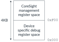
Every CoreSight-compliant component has a 4KB set of debug control registers or a set of debug control registers that are a multiple of 4 KB. Typically, these registers are accessed using an APB interface, though any protocol that can perform device memory type accesses is permissible.
The register space address range is divided between CoreSight component management registers and device-specific Debug registers. The Technical Reference Manual for a CoreSight SoC product defines the device-specific debug control registers for each of the CoreSight SoC components.
ROM Table
This ROM Table on the SoC contains a listing of the components that are connected to the DP or MEM-AP. These listings allow an external debugger or on-chip software to discover the CoreSight devices on the SoC. Systems with more than one debug component must include at least one ROM Table. ROM Tables are connected either to DPs or MEM-Aps A ROM Table entry either contains an address offset for a component on the SoC or a pointer to another ROM Table. You calculate the base address of the component by adding the component address offset to the ROM Table base address. If the ROM Table entry is a component address offset, the PRESENT bit of the ROM Table entry indicates whether the component is present in the system.
Debug Logic inside ARM CORE
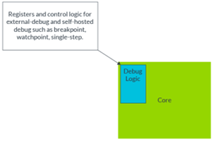
The debug logic that is integrated into an Arm core provides the ability to observe and control the CPU and system environment while executing software on a deeply embedded processor. Control and Access Components Configure, access, and control the generation of trace/Debug. They do not generate traces, nor process the trace data.
What is debug logic?
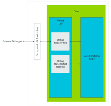
The debug logic of the processor is responsible for generating debug events. Debug logic includes comparators and other hardware logic that enable debug events like breakpoints, single stepping, and watchpoints. Debug logic is fully integrated with an Arm core and is not an entity outside the core.
Depending on the configuration of the debug logic, debug events like breakpoint and watchpoint cause either debug exception or debug state. Let’s look at debug exceptions and debug state in more detail.
- Debug exception: Debug events cause a debug exception if debug logic is configured for self-hosted debug. Debug exception is a synchronous exception that is programmed by the debugger, which is part of the high-level software or operating system. The debugger is also called a self-hosted debugger.
- Debug state: If debug logic is configured for external debug, debug events halt the Processing Element (PE), and the PE enters a debug state. While in the debug state, the PE stops executing the instructions that are pointed by the Program Counter. The PE is controlled by the external debug interface. The external debugger controls the entry of the core into Debug state, by configuring a debug event. A debug event is configured by either programming debug logic, or by asserting a debug halt request through a signal to the core.
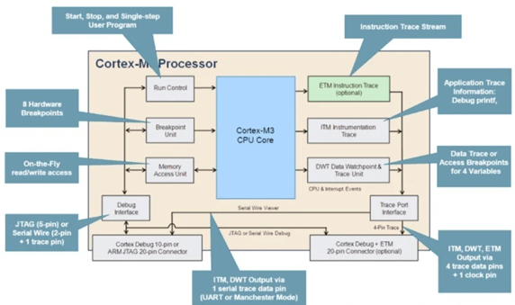
In the Cortex-M3, there can be three types of trace sources:
- Instruction trace: Generated by the Embedded Trace Macrocell (ETM)
- Data trace: Generated by the DWT unit.
- Debug message: Generated by ITM, provides message output such as printf in the debugger graphical user interface.
If you haven’t already, be sure to check out the previous blog in the series, A Complete Guide to SoC Debugging – Part 1 and A Complete Guide to SoC Debugging | Part 2, to build a solid foundation— and stay tuned for the next installment, Part 4: CoreSight-Based Multi-Core.

