- Jintu K Joseph
- May 7, 2025
A Complete Guide to SoC Debugging | Part 4
Debug Trace & Trigger infrastructure
In any complex architecture, debug and instrumentation resources are critical for multicore design. Debug instrumentation provides information for post-silicon debug analysis, software optimization, and performance monitoring.
During the debug phase, the design under debug (DUD) executes normal operations, and the run-time traces of the DUD’s observable points are collected. These traces are analysed for fault detection and localization at the debug analyser. At the beginning of the debug phase, the host system (many a time, the host system and the debug analyzer are the same) configures the trigger unit through the debug port and the debug bus. In the figure, the JTAG interface acts as the debug port, and the configuration channel acts as the debug bus. The trigger configuration is performed to instruct the conditions of triggering. This can be periodic or event-based triggering. Whenever the trigger conditions are satisfied, the trigger happens, and the traces of the observable points are captured. Now, these traces can be transferred to the debug analyser during the run-time through the trace bus and the trace port or can be stored in an embedded trace buffer (ETB) for later analysis. Many a time, the traces are not able to be transferred during run-time due to the bandwidth limitations of the trace bus as well as the trace port. Therefore, trace store and forward methodology is popularly adopted. The width of the CoreSight output trace data bus can be 1, 2, 4, 8, or 16 bits wide. Higher bandwidth output can be obtained using the data packet controller (DPC) high-speed debug port (HSDP). The ATB trace capture is typically achieved using multiple components, including:
Advanced Trace Bus (ATB): A bus used by trace devices to share CoreSight capture resources.
Trace sources: The debug logic is distributed to provide real-time trace facilities for the application processor cores. Below is the list of trace sources introduced by Arm.
- ETM (Embedded Trace Macrocell): The ETM captures detailed information about the executed instructions, providing a complete picture of program flow, including function calls and returns, making it ideal for analyzing complex algorithms or performance bottlenecks.
- ITM (Instrumentation Trace Macrocell): ITM is used to capture custom data points inserted by the programmer through software instrumentation, allowing for logging specific events or variables at specific points in the code. The ITM is an application-driven trace source that supports printf-style debugging to trace Operating System (OS) and application events and emits diagnostic system information. The ITM emits trace information as packets. ITM trace is also called Software trace. The software can write directly to ITM stimulus registers. This emits packets. Timestamps are emitted relative to packets. The ITM contains a 21-bit counter to generate the timestamp.
- DWT (Data Watchpoint and Trace): A watchpoint is a special type of breakpoint that monitors a specific memory tied to a data item. The application pauses execution whenever that memory is modified. The Data Watchpoint and Trace (DWT) unit provides the following: comparators that support watchpoints that cause the processor to enter a Debug state or take a DebugMonitor exception. DWT trace is also called Hardware trace. The DWT generates these packets, and the ITM emits them.
- STM (System Trace Macrocell): The concept behind System Trace Macrocell (STM) trace is that a core can perform data write transactions to a memory-mapped area of the STM, residing on the AXI bus of the processor. This memory-mapped area, called the Stimulus Port, is divided into multiple so-called Channels. A write transaction to such an STM Stimulus Port Channel triggers the STM to emit an STM message via the hardware trace port. The Channel number encoded in the STM message can be used by the trace recording tool to differentiate between different message types. An STM message may contain a data field with a length of up to 64 bits, a timestamp, and also a marker to allow for multi-message protocols, e.g. for sending out strings.
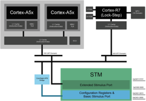
Fig 3: System Trace Macrocell- A Program Trace Macrocell (PTM): This is a real-time module that traces instructions for an Arm core. It can be used to debug programs by providing a record of how instructions are executed. A PTM primarily tracks the flow of program instructions (instruction trace) by marking specific waypoints, while an ETM provides a more detailed trace capturing every single executed instruction, offering deeper insights into the program’s behaviour.
- The Embedded Logic Analyzer (ELA): This is a CoreSight component that monitors signals within a design. The ELA is most commonly used to monitor bus signals. An Embedded Logic Analyzer (ELA) is a debugging tool integrated within a system-on-chip (SoC) that allows developers to monitor specific internal signals within a design, providing detailed insights into the behaviour of various components, particularly useful for pinpointing the root cause of hardware-related issues by observing low-level signal activity during execution; often used to analyze bus signals and memory transactions for debugging complex embedded systems.
- Flash Patch and Breakpoint: The Arm architecture v7-M (1) defines “Flash Patch and Breakpoint” (FPB) as a component that monitors instruction fetch or data read (literal load) to CODE memory in the address range between 0x0 and 0x1FFFFFFF. The FPB provides a mechanism for patching immutable program code or literal constants in firmware by redirecting memory accesses. This is done If an instruction address in CODE memory matches one of the programmable FPB instruction comparators.
- AMBA AHB Trace Macrocell (HTM): The HTM records the AHB activities of the targeted AHB bus and outputs the trace data via the AMBA Trace Bus (ATB) interface. The trace data is then combined with outputs from other trace data sources, such as the Embedded Trace Macrocell (ETM), to generate a unified trace data stream. Depending on the implementation, the trace data can be sent directly to the trace port through the Trace Port Interface Unit (TPIU) or the data can be stored in the Embedded Trace Buffer (ETB).
Trace Link
Trace Funnel: The funnel, also called an ATB funnel, merges multiple ATBs into a single ATB. Typically, the single ATB is then routed to a trace component, for example, another funnel, an ETB, an ETR, or a TPIU. The funnel comes in programmable or non-programmable configurations.
Trace Replicator: In ArmARM CoreSight, a “trace replicator” is a dedicated hardware component that duplicates incoming trace data streams, allowing the same trace information to be sent to multiple destinations simultaneously, essentially acting as a splitter for trace data within the on-chip debug infrastructure; it is useful when you need to send trace information to both an on-chip trace buffer and an off-chip debug interface at the same time.
ATB Bridge: This ATB bridge is used to transport the AMBA trace bus across a power domain boundary.
Trace sinks are the endpoints for the trace data collection on the SoC. There are mainly two types of trace sinks,
- On-chip trace sink: An on-chip trace sink is a component within the debug and trace architecture that captures and stores trace data directly on the chip. Here are some key points about on-chip trace sinks:
- Embedded Trace Buffer (ETB): The ETB is an on-chip memory buffer that stores trace data. It captures trace data from various sources and stores it in a dedicated RAM. The ETB is useful for capturing trace data without the need for external trace storage.
- Embedded Trace Router (ETR): The ETR is another on-chip trace sink that stores trace data across an AXI interconnect. It provides flexibility in routing trace data to different on-chip memory locations.
- Off-chip trace sink: An off-chip trace sink is a component in the debug and trace architecture that captures and stores trace data outside the chip. Here are some key points about off-chip trace sinks:
- Trace Port Interface Unit (TPIU): The TPIU is an ATB (Advanced Trace Bus) slave that drains trace data off the chip. It acts as a bridge between the on-chip trace data and a data stream that is captured by a Trace Port Analyzer (TPA). The TPIU supports off-chip port sizes from 2 to 34 pins.
- Serial Wire Output (SWO): The SWO is a trace sink similar to the TPIU but uses a single-pin interface. It can only trace one source, the Instrumentation Trace Macrocell (ITM), and outputs the data stream off-chip through a single-pin interface.
A Special use case of off-chip trace is trace via PCI express trace port where the trace data is redirected to the PCIE Root complex over the AXI interconnect. A serial trace tool can act then as a PCI Express slave to read the generated trace information. This is especially useful to target with no off-chip trace support.
TPIU: In Arm CoreSight, “TPIU” stands for “Trace Port Interface Unit,” which acts as a bridge between the on-chip trace data generated by the processor’s Embedded Trace Macrocell (ETM) and Instrumentation Trace Macrocell (ITM) and an external Trace Port Analyzer (TPA), essentially allowing the captured trace data to be analyzed off-chip for debugging purposes; it is designed to facilitate low-cost debugging by providing a simple way to access trace information from the processor. The TPIU routes the trace data to external pins. A debugger is connected to these external pins to capture the trace data. The TPIU also adds source identification information into the trace stream so that the trace can be re-associated with its trace source.
TMC: In Arm CoreSight, “TMC” stands for “Trace Memory Controller,” which is a configurable component that allows for capturing and storing trace data from various sources within a system-on-chip (SoC), essentially acting as a buffer to manage the flow of trace information during debugging and analysis. The ArmCoreSight Trace Memory Controller (TMC) is a configurable trace component to terminate trace buses into buffers, and FIFOs, or to route trace data over AXI to memory or off-chip to interface controllers. A TMC has the following three configuration options. In all TMC configurations, an APB interface is also present, to enable runtime control of the TMC behavior.
ETF: Embedded Trace FIFO (ETF) is a component in Arm CoreSight that stores trace data in SRAM. The Embedded Trace FIFO (ETF) contains a dedicated SRAM that can be used as either a circular buffer, a hardware FIFO, or a software FIFO. In circular buffer mode, the ETF has the same functionality as the ETB. In hardware FIFO mode, the ETF is typically used to smooth out fluctuations in the trace data. In software FIFO mode, on-chip software uses the ETF to read out the data over the debug AMBA Peripheral Bus (APB) interface.
ETB: “ETB” stands for “Embedded Trace Buffer,” which is a hardware component within a microcontroller or SoC (System on Chip) designed to capture a chronological record of system events, providing detailed information about program execution flow for debugging purposes, especially in embedded systems where traditional debugging methods might be limited.
ETR: “ETR” stands for “Embedded Trace Router,” which is a component within the Arm CoreSight architecture that acts as a bridge between the trace data generated by a processor and the system memory, effectively routing trace information to a designated memory buffer for later analysis by a debugger; essentially, it allows for capturing large amounts of detailed execution trace data from an embedded system by writing it to a dedicated memory area.
Serial Wire Output (SWO): The trace data from the source is directly passed to an external debugger using a single-wire output called SWO. Owing to the trace bandwidth required, the single-pin SWO is not suitable for outputting the ETM trace data; it is mainly used to pass the ITM data.
Micro Trace Buffer (MTB) trace: Cortex-M0+ devices record changes in the program flow and store trace data packets in a configurable Trace Buffer located in On-Chip SRAM Memory. MTB trace provides simple instruction trace capability for advanced debugging, however, it does not provide time information (time stamps) and data trace capability. MTB runs in a cyclic mode. When the option Stop Trace When Full (or Stop CPU When Full) is left unchecked, the MTB Trace Buffer will be continuously filled meaning once the buffer is full, the new trace information will overwrite the old trace information.
Cross Triggering Infrastructure
Embedded Cross Trigger[ECT] is a mechanism that allows multiple processor subsystems within a System-on-Chip (SoC) to send and receive debug triggers to each other, essentially enabling coordinated debugging across different cores or modules by triggering events on one core based on events happening on another; it is a key component of the Arm CoreSight debug technology.
The ECT consists of two components:
- Cross Trigger Interface (CTI): CTI is Part of an Embedded Cross Trigger (ECT) device. In an ECT, the CTI provides the interface between a processor or ETM and the CTM The CTI combines and maps the trigger requests, and broadcasts them to all other interfaces on the ECT as channel events. When the CTI receives a channel event it maps this onto a trigger output. This enables subsystems to cross-trigger with each other. The receiving and transmitting of triggers are performed through the trigger interface.
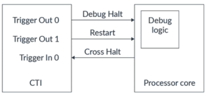
Fig 8: CTI DEBUG IP connection - Cross Trigger Matrix (CTM): This block controls the distribution of channel events. The CTM combines the trigger requests generated by CTIs and broadcasts them to all CTIs as channel triggers. It provides Channel Interfaces (CIs) for connection to either CTIs or CTMs. This enables multiple CTIs to be linked together.
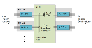
Fig 9: CTM-CTI Channel Protocols
These connections between the CTI and the component are called trigger events. Trigger events are pulses or level-sensitive signals. The Technical Reference Manual for the processor describes the precise trigger event connections between the processor core and the CTI component.
The connections between CTIs through the Cross Trigger Matrix are formed of channels. The matrix consists of four channels: Channel 0, Channel 1, Channel 2, and Channel 3. Each CTI is connected to all four channels. Debug control registers inside the CTI components map trigger event signals to one or more channels. When an input trigger event signal activates, pulses high, or is held high, this activity is propagated along any cross-trigger channel to which the event is mapped. Because the channels connect to all other CTI components, this activity propagates to all other CTI components in the design. When a channel input to a CTI activates, this activity is propagated to any trigger event output to which the channel is mapped. This connectivity through the channels makes it possible for activity on a trigger event input in one CTI component to propagate to the trigger event output of another CTI component.
When a source asserts a trigger, a status bit is set. There are two protocols for managing the status bit. The protocol for each channel is defined in the individual CTI channel tables.
- HW handshake: the source and destination hardware set and clear the trigger status.
- SW acknowledge: that the source sets the status bit with the trigger and the software must clear the status bit.
- For IN ports, write to the source of the trigger.
- For OUT ports, write to the CTIINTACK register.
- There are separate status bits for the IN and OUT ports.
Activity on the signals between the CTI and the processor core can be propagated between the CTI components through this matrix. The CTI contains programmable registers that can be accessed by the debugger to decide which activity to propagate through the matrix. These registers can be programmed so that when one processor core halts, this halting activity is propagated through the CTM components to all the other CTI components in the system, as you can see in the following diagram. The activity is then forwarded to the signal that is used to tell each processor core to halt. This means that when one processor core halts, all the other processor cores should halt soon after. This behaviour is referred to as the cross-hal
If you are an SoC designer, you connect the CTM inside each cluster to the system level where it connects to a system-level CTM. The connectivity to the system-level CTM is what allows the activity at each CTI to propagate through the entire system. The following diagram illustrates how activity in one processor could be distributed to the other processor cores in the cluster and out into the rest of the system through the Cross Trigger Matrix:
It is likely that a debugger device already knows how to program the CTI registers to achieve this cross-halt behaviour. This means that, when using the debugger, you should not need to do low-level programming of the CTI components to achieve the cross-halt. However, the CTI components are not only used for managing the processor halting. The CTI components might be used to generate interrupts or to control trace capture. This means that you might need to tell the debugger how to program the CTI registers to achieve the required behaviour.
Trace output
Trace data is bandwidth-intensive and therefore needs compression/encoding before converting to packets. Therefore, the trace data is not directly in a human-readable format. The trace data when captured by a debugger is decompressed/decoded and processed to convert it to a human-readable format. Sometimes, when transmitting raw data through the ITM, the trace packets can directly have the raw data without encoding. The trace data can be captured in two ways by a debugger:
On-chip capture
In this scenario, the trace data is usually stored in the ETB. At particular points during debugging, the external debugger performs operations to extract the on-chip trace data using a 2-pin serial wire debug (SWD).
Off-chip capture
In this scenario, the trace data is routed to an external debugger in real time using the TPIU and SWO pins. The debugger then processes the data and displays it in a human-readable format. The scope of this application note is mainly to learn this mode of trace capturing.
Case study 1
In this real chip example, we have DAP, AXI AP, and Trace outputs from STM and ETM connected to Funnel. The funnel component arbitrates between the different trace sources. When multiple trace sources attempt to send a transaction in the same cycle, it accepts the transaction from one source and stalls the other transactions. Merging the trace streams into a single bus reduces the area cost of the trace infrastructure. If you are an SoC designer, you can decide to store the trace data on the chip itself inside a dedicated trace RAM. Alternatively, you can send the trace data directly off-chip through a trace port, where it can be captured and analysed directly by a trace port analyser. The standard trace component for sending trace data off-chip is the Trace Port Interface Unit (TPIU). This converts the ATB transactions into a format that can be sent off-chip through a trace port.
Case study 2
In this real chip example, we have an external debugger connected to DAP via a Jtag debug port, 2 Arm cores and 1 non-Arm core, Trace data from each core are merged at the Trace Funnel, it is then routed to the Trace port and On-chip buffer.
If you haven’t already, be sure to check out the previous blog in the series, A Complete Guide to SoC Debugging – Part 1, A Complete Guide to SoC Debugging | Part 2, and A Complete Guide to SoC Debugging | Part 3