- Jintu K Joseph
- March 27, 2025
A Complete Guide to SoC Debugging | Part 1
Introduction
In today’s rapidly advancing world of embedded systems, System-on-Chip (SoC) designs have become a cornerstone of modern electronics, powering everything from smartphones and wearables to automotive systems and industrial IoT devices. The success of these devices relies heavily on efficient development, integration, and debugging of the SoC components.
ARM-based SoCs, with their Cortex-M, Cortex-A, and Cortex-R cores, have emerged as one of the most widely adopted architectures due to their scalability, energy efficiency, and performance. However, designing and verifying these complex systems involves extensive testing and debugging, which is critical to ensuring that the SoC functions correctly under all conditions.
Debugging ARM-based SoCs presents unique challenges due to their multi-core configurations, heterogeneous systems, and varying interfaces. Understanding the debug architecture behind these systems is essential for developers to efficiently detect, troubleshoot, and resolve issues that may arise during both hardware and software development.
In this blog, we will explore the key components and tools used in ARM-based SoC debug architectures, such as JTAG, SWD (Serial Wire Debug), CoreSight, and ETM. We’ll also discuss the importance of real-time tracing, multi-core debugging, and how developers can leverage these advanced debugging capabilities to optimize SoC performance and ensure product reliability.
Whether you are new to SoC development or a seasoned engineer, having a solid understanding of the ARM debug architecture will significantly enhance your ability to design and debug efficient, high-performance SoCs. Let’s dive deeper into how this complex but powerful system works!
Modern SoCs are intricate assemblies comprising various components such as processors, memory blocks, input/output interfaces, and specialized modules. This complexity necessitates robust debugging strategies to ensure functionality and performance.
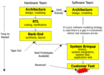
Chip life cycle
The VLSI (Very Large Scale Integration) chip cycle refers to the end-to-end process of designing, verifying, fabricating, and deploying an integrated circuit (IC). The cycle includes multiple phases, ensuring the chip meets performance, power, and area (PPA) requirements while minimizing errors and production costs. The SoC goes through a life cycle as shown below.

To facilitate this product life cycle, debugging is required at different stages, The JTAG/SWD debug interface helps the external debugger to connect and debug the HW. Every system development is a joint effort from the hardware team and software team.
Application-specific integrated circuits (ASICs) are customized chips for specific uses, such as a digital voice recorder or video codec. ASIC development is a complex process that involves many steps and requires a well-defined design flow, similarly, it needs custom and effective software to get the maximum performance.

Debug activities in SOC
- Hardware simulation
- Software simulation
- Hardware-software co-simulation
Simulation-based verification is a crucial step in the design and development of integrated circuits (ICs). Debugging IC requires a combination of best practices and techniques, including a thorough understanding of the design specification, dividing the design into smaller blocks, simulation, test benches, design verification tools, and debugging hardware. It can be challenging and time-consuming, but also rewarding and satisfying. The important technique to find and remove the number of errors/bugs/defects in a program is called Debugging. It is a multi-step process in software development. It involves identifying the bug, finding the source of the bug and correcting the problem to make the program error-free. In software development, the developer can locate the code error in the program and remove it using this process.
Hardware/software co-design is essentially a bottom-up process, where hardware is developed first with a general concept of how it is to be used. Software is then mapped to that hardware. This is sometimes called platform-based design. Co-design is a very good approach to realize highly optimized hardware for a given problem. Hardware-software co-simulation refers to verifying that hardware and software function correctly together. This has traditionally been a task performed after the prototype hardware is available using in-circuit emulators and other techniques. In the case of hardware-software co-verification, the debug architecture plays a crucial role, as it enables the debugger to read out the current status, and configuration at any point in time.
Debugging in any SOC is collectively done using On-chip self-hosted debug and off-chip external debug. On-chip debugging is a combination of hardware and software, both on and off the chip. The part that resides on the chip is implemented in various ways, and for this paper, it will be referenced as On-Chip-Debug (OCD).

Basic On-Chip Debugging (OCD) allows for code download, reading and writing memory and processor resources, single stepping, processor reset, and status (running or halted). Typically, on-chip peripherals may be set to shut down during OCD. GDB [Gnu Debugger] communicates with a debug adapter directly over ethernet using RSP protocol or using OpenOCD.
To enable on-chip debugging, you need two main components: a debug interface and a debug tool. The debug interface is a hardware module that connects the SoC to the debug tool. It can be either embedded in the SoC or attached as a separate chip.
Challenges of SoC debugging
- Debug Visibility: A crucial aspect of SoC debugging is to have enough visibility into the internal state and behaviour of the chip, which enables identifying and fixing the root causes of the errors. However, debug visibility is often limited by the lack of observability and controllability of the internal signals, the complexity and diversity of the software and hardware components, and the trade-offs between debug features and design constraints. To avoid this pitfall, you should use debug architectures and tools that provide adequate and flexible access to the internal signals, such as scan chains, trace buffers, debug registers, and debug buses.
- Debug Scalability: Another challenge of SoC debugging is to scale up the debug process to handle the increasing size and complexity of the SoCs, which involve more components, more interactions, more errors, and more data. Debug scalability depends on factors such as the debug architecture, the debug tools, the debug data, and the debug expertise.
- Debug Quality: The goal of SoC debugging is to ensure the quality of the SoC, which means meeting the functional and non-functional requirements and specifications of the system.
SoC designers are aware of the need for a bug-free hardware design, a processor with sufficient performance and the need to tape out on time. But the need to fit the best debug logic is not always uppermost in their mind.
Challenges in SOC Design
Designing a System-on-Chip (SoC) can be quite challenging, and several common issues are often encountered during the process:
- Power Consumption: Managing power consumption is critical, especially for portable devices with limited battery life. Techniques like power gating, voltage scaling, and clock gating are used to reduce power consumption.
- Design Complexity: SoCs integrate multiple components such as CPUs, GPUs, memory, and communication interfaces, making the design process complex. Efficient algorithms, optimized architecture, and advanced design tools are essential to manage this complexity.
- Verification and Testing: Ensuring that the SoC functions correctly under various conditions requires comprehensive verification and testing. This includes developing extensive test benches and simulation environments.
- Performance: Balancing performance with power efficiency is a significant challenge. SoC designers must optimize the architecture and use advanced design techniques to meet performance requirements.
- Security: With increasing connectivity, security has become a critical concern. SoCs must be tested against security threats such as hardware Trojans, side-channel attacks, and secure boot mechanisms.
- Integration: Integrating various IP blocks and ensuring they work together harmoniously is a complex task. This requires careful planning and verification.
- Signal Integrity: Maintaining signal integrity, especially at high frequencies, is crucial for reliable operation. This involves careful design of the interconnects and proper layout techniques.
Test and debug requirements.
- Software and application debug: Here apart from the traditional individual processor-based debug, provisions for non-intrusive access to register and memory space during run time should exist.
- Break points: We should have provisions to enter a debug space either from a software event (software source-level debugging) or a hardware event (enter into debug mode based on a hardware event such as interrupts, bus transactions etc.)
- Synchronized debugging: We should have provisions to enable synchronized debugging between processors. Further, it is desirable for not only synchronize processors during debugging but also SoC peripheral events generated such as timer events, hardware interrupts and bus transaction events.
- Silicon test and debug: Here we look for a standardized communication interface between the tester ATE (Automatic Test Equipment) and the SoC so that the tester can control, load test vectors, and observe the results efficiently. Interfaces like JTAG may become the preferred interface.
- Secure access: Many times, the debug interface may be used by hackers to gain access to the SoC and steal many intellectual properties, or enable alternative use of the SoC (e.g. Xbox used as a cheap Linux computer). Provision should be in place to avoid unauthorized access to the SoC.
- Debug hardware: While designing a debug solution care should be taken that only minimum hardware real estate and pins are used for debugging. If the real estate for debugging is more than two to three per cent of total IC real estate, then it becomes very difficult to sell the idea of debugging for commercial reasons.
- Efficient debug access: Traditionally a JTAG interface is used as a debug access mechanism. Here there could be two ways of accessing the SoC resources. One is through the traditional processor debug port and the second one is to have a direct JTAG to the system bus.
Debug support for SOC
The debugger can be used to identify if the program is running correctly and identify the cause of failure when it fails. The debugger may be a source-level debugger or a low-level debugger. If it is a source-level debugger, the debugger can show the actual position in the original code, when the program crashes. If it is a low-level debugger or a machine-language debugger, it shows that line in the program. Catching run-time errors is not as obvious. Most embedded systems do not have a “screen”. Hence, we cannot find the run time errors as in general software development.
Remote Debugger is used to monitor/control embedded SW. It is used to download, execute, and debug embedded software over a communications link. The program running on the host of a remote debugger has a user interface that looks just like any other debugger that you might have used. The main debugger screen is usually either a command-line interface or a graphical user interface (GUI). GUI debuggers typically contain several smaller windows to simultaneously show the active part of the source code, current register contents, and other relevant information about the executing program. Note that in the case of embedded systems, the debugger and the software being debugged are executed on two different computer systems.
Hardware support for debugging
Suitable hardware architecture is required to facilitate the debugging. This can be done using the CoreSight™ SoC components to design a suitable debug subsystem. A typical debugger device controls the JTAG or serial wire transactions and target accesses at the Debug registers inside the device. This means that, when you use a debugger, you only need to decide which debug logic you want to use inside the processor cores to help debug the malfunctioning software program. You do not need to do low-level programming of CoreSight™ components from the debugger.
If you are an SoC designer, you might decide to provide debug access to the APB protocol bus using functional IOs, instead of using a JTAG or Serial Wire Debug Port to provide the off-chip debug access. That is, you might be able to repurpose some of the device’s functional connectivity and use that connectivity for debug purposes. The advantage of this approach is that dedicated IOs for debugging purposes are not required. Debugging could be allowed from a non-standard debugging source, for example, using software routines that are running on a PC and connecting to the device using a USB port. However, this approach requires the development of design-specific debug connectivity and software. This approach is typically followed when an SoC designer is considering a specific debug scenario.
Every Arm processor core has some debug functionality that is built in. This debug functionality is used in two general modes:
- Self-hosted Debug: In which code that is running on the processor core uses the debug capability to identify problems in the software.
- External Debug: in which an external debugging component, the debugger, can access the debug features and use them to identify problems with the software.
W.r.t to external debug, it is again classified as follows:
- Invasive debug: In this type of debug the debugger will interact with the processor by halting it.
- Non-invasive debug: The memory content and peripheral registers can be examined even when the processor is running.
- Run control debugging: This type of debugging allows external hardware and software to access and control CPUs. Run-control debugging uses JTAG and some sideband signals. Examples of emulator hardware include Intel® In-Target Probe (ITP) and ASSET Arium ECM-XDP3e probe. Run-control is used to stop and start processors, read and write registers, I/O and memory, and perform such functions as setting breakpoints and single-stepping through code.
Concurrent software distributed across multiple CPUs and hardware accelerators, interacting with complex I/O interfaces and strict real-time requirements is the new normal. This results in new classes of bugs which are hard to find, like race conditions, deadlocks, and severely degraded performance for no obvious reason. To find such bugs, run-control debugging is not applicable: setting a breakpoint disturbs the temporal relationship between the different threads of execution. Tracing avoids these problems by unobtrusively monitoring the program execution and transferring the observations off-chip.
Many smaller single-core designs traditionally only support run-control debugging through custom JTAG-based debug infrastructure. Examples of debugging applications which use this hardware are the Intel Platform Debug Toolkit (PDT) and ASSET SourcePoint debugger.
Debug probe options
Debug provides the ability to observe and control the CPU and system environment while executing software on a deeply embedded processor. The ability to debug helps to fix bugs in the software and to optimize the software for performance. The debug logic that is an integrated part of the Arm cores helps to achieve these goals. An External debugger typically interacts with a processor via an independent debugging interface. Most software debuggers use IEEE 1149.1 JTAG & and Serial Wire Debug.

Typically, external debuggers use the JTAG (IEEE 1149.1) or serial wire debug protocols to provide the connection to the chip. These protocols are used because they limit the number of pins that are required, which helps reduce the physical cost of the debug infrastructure. Once the JTAG or serial wire transactions are on the chip, they are converted into parallel bus transactions.

Debug modules (shown on the right) monitor or interact with the functional components of the SoC. Towards the functional SoC, the interface is implementation-specific. Towards the debug interconnect the modules conform to a standardized interface, which is specified in this document. The debug interconnect is used to exchange data between debug modules and between the target and the host. The format of the data transmitted over the debug interconnect also conforms to a standard. Debug tools use the debug system to perform debugging and analysis tasks, ranging from run-control debugging to tracing and runtime verification.
1. Future Technology Devices International (FTDI): Future Technology Devices International (FTDI) is a Scotland-based semiconductor company specializing in USB-to-serial interface solutions and embedded hardware. FTDI is widely known for its USB-to-UART bridge chips, which simplify communication between microcontrollers and computers, replacing legacy RS-232 serial ports.
2. CMSIS-DAP: CMSIS-DAP is an open-source debug protocol developed by ARM to provide a standardized USB-to-debug interface for ARM Cortex-M microcontrollers. It allows a debugger (host computer) to communicate with a target MCU via SWD (Serial Wire Debug) or JTAG, using a USB-based debug probe.

3. SEGGER J-Link Debug Probe: SEGGER J-Link is a high-performance debug probe widely used for debugging, programming, and tracing ARM Cortex-M, RISC-V, and other microcontrollers. It supports JTAG, SWD (Serial Wire Debug), and SWO (Serial Wire Output), offering fast and reliable debugging with professional tools like Keil, IAR, GDB, and SEGGER Embedded Studio.

Stay tuned for Part 2 of A Complete Guide to SoC Debugging, where we’ll break down hardware debugging interfaces like JTAG and SWD, and help you choose the right interface for your needs!