- Benetta Peter and Nevil Alex
- June 22, 2022
Intelligent clock calibration based TDM for multi-FPGA emulation
SoC re-spins can mostly be attributed to functional errors that are introduced during the RTL coding phase of the design process. Hardware simulations lower the risk of such design errors. However, given the increased size and complexity of designs, simulations are slow and often do not provide enough coverage to ensure the design is bug free. FPGA-based emulation has proved to be extremely beneficial in guaranteeing silicon success and for early development of software in SoC design cycles. FPGA based emulation can be done at clock frequencies that are a tenth or a twentieth of ASIC clock frequencies and therefore real-time performance can easily be measured and complex software can easily be tested using this platform. And with exponential increase in size of VLSI design, the designs are now partitioned among multiple FPGAs for emulation purposes.
Multi-FPGA Emulation
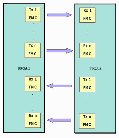
In order to implement larger designs, we use multi-FPGA system, which is a collection of FPGAs that are interconnected by physical cables for intercommunication between FPGAs. Interconnection lines are normally high-speed capable. All the wires in the cable should be of same length to ensure that timings are matched appropriately outside the FPGA. Furthermore, the FPGA board should have the appropriate connectors like FMC connectors through which multiple signals can be sent. The number of signals transmitted between the FPGAs depends on number of connectors and number of pins available in each connector. However, most FPGA boards have limitation of fewer I/O pin availability. As a result, input/output time-division multiplexing (TDM) is used to deliver a collection of cross-FPGA signals in a single routing channel.
Time Division Multiplexing (TDM)
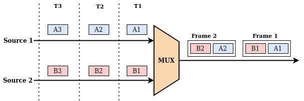
TDM allows multiple data signals to be transmitted across same data channel at different time slots. The input signals from different data sources are divided into multiple frames at fixed length time slots and are multiplexed. Each data frame at the output of multiplexer consists of one data unit from each input source. At the receiving end, demultiplexer will reassemble the frame back to the complete signal.
The figures show 2×1 multiplexer and its waveform. This can be extended to nx1, where n should be in powers of 2. For a nx1 multiplexer, the frequency of TDM mux signals will be n times that of input signals.


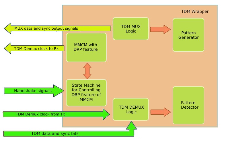
The set of data signals and the required TDM handshaking signals are passed through each FMC group. In this mode of inter-FPGA communication, the variable delay associated with individual wires in different FMC-to-FMC connectors and variable I/O delays can result in data corruption at receiving end. This issue is eliminated by enabling dynamic reconfiguration feature for demux clock at the receiving end.

The number of data signals in each group can be configured depending upon the FMC connector’s pin count. The TDM ratio is decided based on the I/O pin availability in the FPGA and in the design. The TDM calibration phase is carried out with known test patterns to identify the demux clock phases over which TDM data is correctly demultiplexed at receiver end. The calibration algorithm ensures that the phase selected for mission mode operations is at the center of the eye for accurate and reliable communications.

A LUT based pattern generator logic can be implemented to generate test patterns at Tx FPGA for TDM calibration process. A pattern detector logic ensures the correctness of received pattern at Rx FPGA. At transmitter side FPGA, a set of known test patterns is generated and is multiplexed in each TDM group and sent out to receiver side FPGA. At Rx side, this pattern is De-muxed back and is compared against the test pattern for each group. Any mismatch will raise separate error flags for each group. If the pattern is correctly received, then a TDM handshake signal is asserted high to indicate the same and is sent back to the Tx side. This is repeated for demux clock with multiple clock phases and median of locked phases are calculated.
Conclusion
FPGA Emulation serves as a catalyst for software development and helps in developing high confidence in the quality of silicon. With larger silicon footprints, FPGA partitioning and therefore multiplexing of FPGA IOs is almost mandatory in emulation cycles. A calibration-based strategy for IO multiplexing ensures that the same design can be used across FPGA platforms as it is agnostic to variability in IO and wire delays. This ensures robustness in the design approach and can lead to productivity improvements by saving on the bring up time for FPGA emulation.


